

Analysis and Processing of Transmission Line Effect in High Speed Circuits
With the large-scale improvement of system design complexity and integration, electronic system designers are engaged in circuit design above 100MHZ. Bus frequency has reached or exceeded 50MHZ, and most of them even exceed 100MHZ. At present, about 80% of the design clock frequencies exceed 50MHz, nearly 50% of the design main frequencies exceed 120MHz, and 20% even exceed 500M.
When the system works at 50MHz, the transmission line effect and signal integrity problems will arise. When the system clock reaches 120MHz, the PCB designed based on traditional methods will not work unless the knowledge of high-speed circuit design is used. Therefore, high-speed circuit signal quality simulation has become a necessary design method for electronic system designers. Only through high-speed circuit simulation and advanced physical design software can the controllability of the design process be realized.
Transmission line effect
Based on the transmission line model defined above, it can be concluded that the transmission line will bring the following effects to the whole circuit design.
· Reflected signals
· Delay & Timing errors
· Overshoot/Undershoot
· Induced Noise (Crosstalk)
· EMI radiation
1. Reflected signals
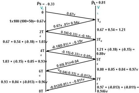
In high-speed circuits, the transmission of signals is shown in the figure. If a line is not terminated correctly (terminal matching), the signal pulse from the driver is reflected at the receiver, which causes an unpredictable effect and distorts the signal contour. When the distortion distortion is very significant, it can lead to many kinds of errors and design failure. At the same time, the sensitivity of distorted signal to noise increases, which will also lead to design failure. If the above situation is not considered enough, EMI will increase significantly, which will not only affect the design results, but also cause the failure of the whole system.
The main reasons for the reflection signal are: too long line, unmatched transmission line, excessive capacitance or inductance and impedance mismatch.
2. Delay & Timing errors
The performance of signal delay and timing error is that the signal keeps unchanged for a period of time when the logic level changes between high and low threshold. Excessive signal delay may lead to timing errors and confusion of device functions.
Usually problems occur when there are multiple receivers. Circuit designers must determine the worst-case time delay to ensure the correctness of the design. Reasons for signal delay: drive overload, long line.
3. Overshoot/Undershoot
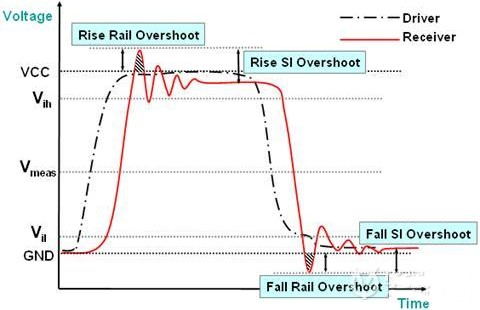
The overshoot comes from two reasons: too long line or too fast signal change. Although most component receivers are protected by input protection diodes, sometimes these overshoot levels can exceed the component power supply voltage range and damage components.
4. Induced Noise (Crosstalk)
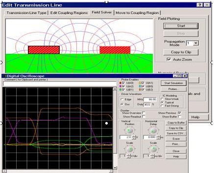
Crosstalk is that when a signal passes through a signal line, the signal will be sensed on the adjacent signal line on the PCB board. We call it crosstalk.
The closer the signal line is to the ground line, the larger the distance between the lines, the smaller the crosstalk signal. Asynchronous signals and clock signals are more likely to produce crosstalk. Therefore, the method of de-crosstalk is to move the crosstalk signal or shield the seriously disturbed signal.
5. EMI radiation
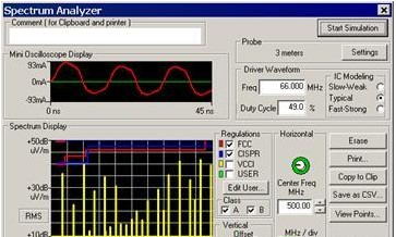
EMI is electromagnetic interference. The problems caused by EMI include excessive electromagnetic radiation and sensitivity to electromagnetic radiation. EMI shows that when the digital system is powered up, it will radiate electromagnetic waves to the surrounding environment, thus interfering with the normal operation of electronic equipment in the surrounding environment. The main reason is that the circuit working frequency is too high and the layout and wiring are unreasonable. At present, there are software tools for EMI simulation, but EMI simulators are very expensive, and it is difficult to set simulation parameters and boundary conditions, which will directly affect the accuracy and practicability of simulation results. The most common way is to apply the design rules that control EMI to every link of design, and to realize the rule driving and control in every link of design.
Method of Avoiding Transmission Line Effect
In view of the impact of the above transmission line problems, we will discuss the methods to control these impacts from the following aspects.
1. Strictly control the routing length of key wires
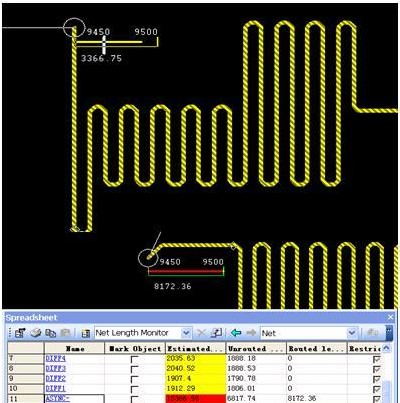
If there is a high-speed jumping edge in the design, the transmission line effect on the PCB board must be considered. This is especially true of fast integrated circuit chips with high clock frequencies, which are widely used nowadays. There are some basic principles to solve this problem: if CMOS or TTL circuit is used for design, the working frequency is less than 10MHz, and the wiring length should be less than 7 inches. The wiring length at 50MHz should not be more than 1.5 inches. If the operating frequency reaches or exceeds 75MHz, the wiring length should be 1 inch. The maximum wiring length for GaAs chips should be 0.3 inches. If this standard is exceeded, the route should be located by software simulation. The exact length of the route should be controlled by physical software (such as PADS, etc.).
2. The Topological Structure of Reasonable Planning Routing
Another way to solve the transmission line effect is to select the correct route and terminal topology. When using high-speed logic devices, unless the branch length of the line remains very short, the fast-changing signal along the edge will be distorted by the branch line of the signal backbone. Usually, PCB routing uses two basic topological structures, namely Daisy Chain routing and Star distribution.
For chrysanthemum chain routing, the routing starts at the driver end and arrives at each receiving end in turn. If the series resistance is used to change the signal characteristics, the position of the series resistance should be close to the driving end. The chrysanthemum chain has the best effect in controlling the high-order harmonic interference. But this routing method has the lowest routing rate, and it is not easy to get 100% routing. In practical design, we make the branch length of chrysanthemum chain as short as possible, and the safe length should be Stub Delay <= Trt * 0.1.
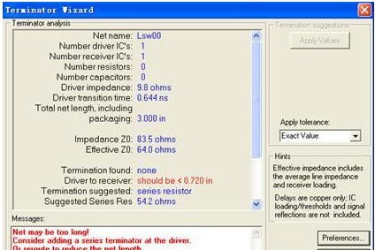
Star topology can effectively avoid the problem of clock asynchronization, but it is very difficult to finish routing manually on high density PCB board. Using automatic wiring device is the best way to complete star wiring. Terminal resistance is required on each branch. The resistance of the terminal resistance should match the characteristic impedance of the line. The characteristic impedance and terminal matching resistance can be calculated by software simulation.
3. Methods of Suppressing EMI
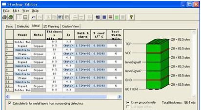
Solving the signal integrity problem well will improve the electromagnetic compatibility (EMC) of PCB board. It is very important to ensure that the PCB board has a good grounding. It is very effective to use a signal layer and a ground layer for complex design. In addition, minimizing the density of the outermost signal of the circuit board is also a good way to reduce electromagnetic radiation. This method can be realized by using the "Build-up" technology to design PCB. Surface layer is realized by adding thin insulating layer on common process PCB and the combination of micro-holes used to penetrate these layers. Resistance and capacitance can be buried under the surface layer, and the line density per unit area will increase nearly twice, thus the volume of PCB can be reduced. The reduction of PCB area has a tremendous impact on the topological structure of the route, which means that the current loop is reduced and the branch line length is reduced, while the electromagnetic radiation is approximately proportional to the area of the current loop; at the same time, the small size feature means that the high density pin packaging device can be used, which in turn reduces the length of the connection and thus electrically generates electricity. The current loop decreases and the EMC characteristics are improved.
4. Other Available Technologies
Decoupling capacitors should be added to IC chips in order to reduce the instantaneous voltage overshoot on the power supply of IC chips. This can effectively remove the impact of burrs on the power supply and reduce the radiation of the power loop on the printed circuit board.
When the decoupling capacitor is directly connected to the leg of the power supply rather than to the power supply layer of the integrated circuit, the effect of smoothing burrs is the best. This is why some devices have decoupled capacitors on their sockets, while others require that the distance between the decoupled capacitors and the devices be small enough.
Any high-speed and high-power devices should be placed together as far as possible to reduce the instantaneous overshoot of power supply voltage.
If there is no power supply layer, then the long power supply wiring will form a loop between the signal and the circuit, and become a radiator and easy induction circuit.
The circumstance that a route constitutes a loop that does not pass through the same network or other routes is called an open loop. If the loop passes through other routes of the same network line, it forms a closed loop. Antenna effect (wire antenna and ring antenna) can be formed in both cases. The antenna produces EMI radiation to the outside, and it is also a sensitive circuit. Closed-loop is a problem that must be considered because its radiation is approximately proportional to the area of the closed-loop.
To implement all the empirical methods mentioned above, manual calculation can not be completed, which is controlled by software simulation and EDA software.



