

Signal Integrity in High Speed Circuit Board Design
Signal Integrity (SI) is becoming a growing concern of digital hardware designers. With the increase of data rate bandwidth in wireless base stations, wireless network controllers, wired network infrastructure and Military Avionics systems, the design of circuit boards has become increasingly complex.
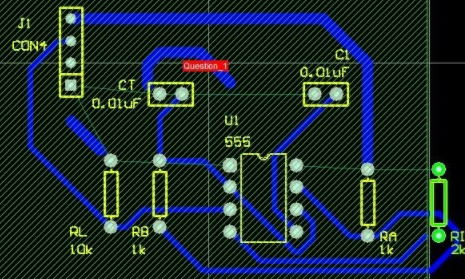
This paper mainly discusses the signal integrity problems related to high-speed interface design (the main functions of RapidIO switching support these high-speed interface design) and other related issues. The purpose of optimizing RapidIO switching function is to achieve high signal integrity in high-speed design.
Difficulties in High Speed Interface Design
Signal quality is very important for all aspects of the system. For serial RapidIO, signal quality is quantified by the size of the received eye image. Receiving eye diagram is an infinite continuous trajectory in which the waveform repeats with the previous trajectory. The bigger the eye chart, the better the signal quality.
Signal quality may be affected by many factors: noise or other cluttered signals in signal channels, poor wiring of signal channels, conduction or radiation of external sources, noise generated by the system itself. Combining all the above factors will result in the shrinkage of the receiving eye diagram. In addition to circuit board level problems, signal integrity may also be affected by the source (transmitter) and destination (receiver) of the connection. Therefore, the IC characteristics of source and destination should be considered in the signal integrity of the whole system level.
Considerations in PCB Level Design
In terms of circuit board design, common factors to be considered include:
1. Power Input of PCB, Output and Distribution of Local Regulator
2. Clock Generation and Allocation
3. Decoupling
4. PCB Foundation Materials
5. Interchip Connection
6. Intercircuit Board Connection and Backplane Connection
7. Circuit Board Lamination and Impedance Control
8. Interrack connectors, cables and connectors
When the operating frequency is higher than 300 MHz, most design best practices for lower frequency circuit board design need to be modified. Consideration must be given to factors that occur when the wavelength is comparable to the size of the circuit board. This is not only applicable to the wavelength of the basic frequency, but also to the Fourier component of the complete waveform.
FR4 material can still be used as the basic material of circuit board successfully, but at higher frequencies, not only dielectric constant but also loss coefficient need to be considered. The design of through holes has also become very important, because the impedance of unused tube lengths (which can be neglected at lower frequencies) will not match the impedance of thicker circuit boards and backboards. It is better to complete the post-design simulation to draw attention to the less ideal wiring of signal integrity and point out the crosstalk area.
The specific problems of signal integrity on circuit boards are caused by the existence of high-speed processor bus and high-speed memory interface, clock generation, clock noise and various noise sources on circuit boards, usually including single-ended parallel bus, power distribution, impedance matching, ground bounce, crosstalk and clock generation.
Serial RapidIO Switch
Serial RapidIO interconnection can be used to deal with some of the signal integrity problems discussed above. RapidIO is a mature and open standard for interconnection among chips, circuit boards and chassis. It is designed by leading manufacturers in embedded computing. It can meet the requirements of reliability, cost-effectiveness, performance and scalability of equipment in wireless infrastructure, network, storage, science, military and industrial markets.
RapidIO is a point-to-point data packet switching interconnection protocol designed to meet the needs of current and future embedded applications. RapidIO Physical Layer 1 x/4x Link Serial Specification can meet the physical layer media requirements of devices using electronic serial connections. The specification defines a full duplex serial physical layer interface (link) between devices using one-way differential signals. In addition, it allows four serial links to be combined for applications requiring higher link performance. It also defines protocols for link management and data transmission through links.
The architecture of RapidIO system consists of endpoint components and switching structures connecting endpoints. Imagine an endpoint as the starting point in a mail system, and a switch as the post office where the package is intercepted and sent to the destination. RapidIO interconnection architecture is divided into layered architecture according to specifications, including logical layer, common transport layer and physical layer. The physical layer of RapidIO protocol is handled by the chip serializer-serializer (SerDes). The characteristics of SerDes have a certain impact on the signal integrity problems faced by hardware designers when designing circuit boards. Many other aspects of switch design will also affect signal integrity.
RapidIO switching simplifies circuit board design and achieves high signal integrity
Clock Generation
For starters, sRIO switches must have noise-free clock signals to achieve low jitter. Low jitter signal basically has the characteristics of low phase noise. If the input clock signal is added to achieve higher frequency output signal, the chip circuit must be optimized to generate minimum phase noise. Tundra's Tsi57x Serial RapdIO Switch generates up to 3.125 Ghz output signals by using integrated low noise amplification PLL's 125 MHz and 155 MHz clocks. Many products use independent circuits to achieve the above functions, which makes it impossible to achieve low jitter like Tundra switching chip. The clarity of the output signal is not as good as that of the Tundra switching chip, which makes it difficult for the circuit board design to tolerate other board-level signal integrity issues discussed above.
Programmable transmission pre-emphasis and receiver equalization
In the design of high-speed circuit board, the attenuation of signal needs to be considered because the signal is transmitted from the chip to the chip or through the backplane through the circuit board. In short, the actual signal strength decreases when it reaches the endpoint, and phase shift may occur. Usually, in all media, high frequency harmonics have a larger proportion of attenuation than low frequency harmonics. Enhancing the overall signal is not enough because it enlarges the noise layer and does not solve the phase shift problem. Serial RapidIO switching and endpoints (like all other high-speed designs such as GbE and 10GbE) utilize technology to avoid this problem and maintain the integrity of the original signal.
To understand the effects of transmission pre-emphasis and receiver equalization, you can review eye maps, the goal of which is to achieve "eye opening". If these techniques are not used, eye maps will begin to "close".
The transmission pre-emphasis technology can add high frequency to the transmission signal to solve the problem of signal attenuation and phase shift between endpoints. Therefore, unlike simply amplifying all frequencies (which also increases the overall power consumption of the switching chip), transmission pre-emphasis can effectively enhance the output waveform and increase the high frequency of the output waveform through transmission function, while using virtual components to phase-shift it to solve the phase-shift caused by transmission media. This method is very effective for preserving the integrity of the signal and keeping the eye diagram.
Although transmission pre-emphasis is usually used in many high-speed IC applications to optimize the overall system-level signal integrity, the transmission pre-emphasis of the "transmission end" should be used in conjunction with the receiver of the "receiver end". Receiver equalization uses the enhanced transmission function to compensate the high frequency transmission loss and phase shift caused by circuit board and backplane. Since these transmission losses occur before the signal arrives at the destination IC (in this article, serial RapidIO switching), the switch must take measures to compensate for these losses before the signal is sent to the next transmission part (another switching) or endpoint in the system. Receiver equalization is similar to transmission pre-emphasis, which can improve the overall signal-to-noise ratio. Note: Links to switch chips may have different characteristics.
Similarly, the equalization needs of the links will vary and need to be programmed before they can be used. All Tundra RapidIO Tsi57x exchanges have this feature. As far as signal integrity is concerned, this feature will greatly simplify system-level design.
Design of synchronous and asynchronous switching
The serial RapidIO standard supports three different link rates: 1.25G Port, 2.5G Port and 3.125G Port. Switching can be divided into two categories: synchronous and asynchronous.
Synchronized switching means that all ports must operate at the same speed.
Asynchronous switching refers to the switching that each port can operate at the frequency required by the traffic demand of a specific link.
In most applications, the best solution is asynchronous switching, which not only has the advantage of satisfying the traffic demand with lower overall power consumption of the system, but also is less affected by crosstalk in terms of signal integrity.
Packaging and Interconnection
Signal integrity problems may be largely affected by packaging and basic material design. For example, high performance flip chip and wiring connection package can improve power transmission and reduce return loss. For RapidIO switches, it is important to improve impedance matching to maintain 100 ohm differential impedance and lower variation. Flip chip packaging can help to improve the above situation.
Efficient spherical mapping
Silicon wafer suppliers may choose spherical mapping to simplify signal transmission from chip to grid, but its role is not limited to this. Ideally, global system-level implementation is considered when designing spherical mappings. For example, when designing spherical mappings, it is important to remember to link peripheral ICs to switching chips. The design should be optimized to minimize the number of layers and required area, which can improve the signal integrity of the final design. IC with fairly dense spherical mapping requires many layers on the circuit board to send signals from IC, resulting in high-cost system-level design. Another problem is crosstalk between signaling channels, which was mentioned above when discussing the difference between synchronous and asynchronous RapidIO switching. One of the problems closely related to crosstalk between signal channels and efficient spherical mapping is the gap between the power supply and the ground pin. If too many serial RapidIO ports are inserted into small packages, the problem of signal integrity may be caused by crosstalk, resulting in "closed eyes" when the signal is transmitted from the switch to the end point.
Design Practice Skills
Now, let's review another aspect of signal integrity, that is, circuit board level design. Designers can adopt many design guidelines to control the impact of noise. Usually, good design practices can help circuit board designers control the signal noise generated by board-level communication, including limiting external noise sources and resolving the noise of the equipment itself.
Firstly, all designs should adopt correct widths, spacing and topologies to ensure that the impedance of each route matches its transmission device. Impedance mismatch may affect the quality of leading edge and trailing edge, stability delay time, crosstalk and EMI.
Sufficient channel spacing between synchronous signal groups must be ensured, channel length must be limited and differential offset between signals must be minimized. In order to limit parasitic effect, the number of routing layer switching should be minimized. The cost of passing holes in unnecessary inductors and stray capacitors is very high and should be reduced as much as possible. In addition to BGA gaskets, usually each channel is allowed to have at most two through holes.
Complete verification of signal integrity is crucial. By estimating parasitic effects, pre-design analysis can provide the data needed to understand design performance, but accurate post-design parasitic effects can provide the details needed to identify potential signal integrity problems. With this method, a circuit network table can be created to simulate and record the results.
If the channel and signal channel are shortened as far as possible, shielded by grounding layer or physical isolation from each other, and avoided impedance mismatch or any configuration leading to resonance, good signal integrity can be achieved.
Selecting Serial RapidIO Switching Chip to Realize Higher Signal Integrity
How do designers choose serial RapidIO switching? Just as good design practices can help circuit board designers control the signal noise generated by board-level communication, hardware designers need to actively consider the characteristics of clock generation, transmission pre-emphasis and receiver equalization, optimization of packaging technology, effective spherical mapping and differences. The step-by-step design of serial RapidIO switch can ensure that the system-level design has high signal integrity. Obviously, when choosing the serial interface, the chip chosen by the designer not only has the appropriate function, but also must be a switch chip specially designed to solve the problem of high-speed signal.
At present, Tundra Semiconductor Corporation can provide three generations of serial RapidIO switching products with the above characteristics. The Tsi 57x product line includes Tsi574, Tsi576 and Tsi578. The number of ports varies from 4 to 16 ports, and the operation speed ranges from 1.25G to 3.125G. Each port supports X1 and X4 channels with power consumption of 120 to 200 mW. The Tsi57x product line has all the signal integrity characteristics described in this paper, including transmission pre-emphasis and receiver equalization. Compared with the previous Tsi56x product line, this product adds some new functions, including multicast function and matrix performance monitoring. In addition, many advanced communication management functions have been optimized to meet the high performance requirements of applications such as wireless base stations, wireless network controllers, wired network infrastructure and Military Avionics systems.
Summary of this article
Through the above analysis, we can find that if we are familiar with the basic design rules, we can avoid any traditional problems related to poor signal integrity when applying high frequency interconnection (such as serial RapidIO) in the system, such as noise, instantaneous effect, crosstalk or jitter, etc.



